The good joint: shiny, concave, fully wetted
A good through-hole solder joint looks like a small, shiny, concave cone wrapped around the lead. Three properties, no exceptions:
The three properties
- Shiny. The surface should reflect light cleanly. A good joint cooled smoothly from molten solder; the surface tension during cooling pulls it into a clean reflective skin.
- Concave fillet. The shape — viewed from the side — is a cone or fillet that narrows from the pad up to the lead. Concave, not bulging outward. A blob of solder sitting on top of the pad is wrong even if it looks "complete".
- Fully wetted. The solder is in contact with the entire annular ring of the pad and the lead, on both top and bottom of the board. You can see the pad-to-lead transition through the solder; it's not just a ball perched on top.
What "wetting" means
Wetting is the chemical and physical bond between molten solder, the copper pad, and the metal of the lead. When solder wets properly, the molecules grip both surfaces and form a real connection — mechanical, thermal, and electrical, all in one.
When solder doesn't wet, it sits as a separate ball on top, held in place by gravity. The connection looks complete but isn't; it'll fail mechanically (any vibration breaks it) or electrically (high resistance, voltage drop, signal integrity issues).
The recipe for a good joint
- Place the lead through the pad. Lead should protrude 1-2 mm below the pad on the solder side.
- Touch the iron tip to both the pad and the lead simultaneously. Heat the joint, not just the solder.
- Wait ~1 second for the heat to transfer, then touch the solder wire to the joint (not the iron).
- Solder flows into the joint as it melts, drawn by capillary action up around the lead. You'll see the fillet form.
- Remove the solder, then remove the iron. Total contact: typically 2-3 seconds for through-hole on a standard PCB.
That's it. Heat the joint, feed solder into the joint, watch it wet, remove. The next slide covers what defects look like when one of those steps goes wrong.
Common defects: cold, blobby, bridged
Most soldering problems look obvious once you've seen them named. Here's the four defects you'll see most often and what causes them.
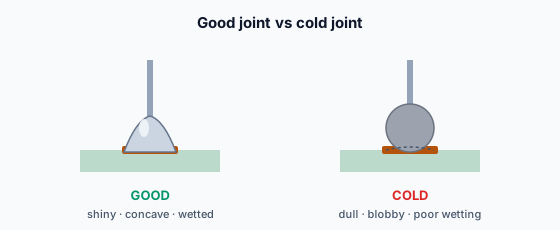
Cold joint
Looks: dull, grainy, sometimes cracked. Not the clean shiny surface of a good joint.
Cause: the joint moved while solidifying, or the iron wasn't hot enough to keep the solder molten long enough to wet the pad and lead. The solder froze partly wetted, partly not.
Fix: reflow. Touch the iron back to the joint, let the solder remelt, give it a moment, lift the iron and let it cool undisturbed. If it's still dull, add a tiny bit of fresh solder (with flux) to give it room to reflow cleanly.
Solder ball / blob (insufficient wetting)
Looks: a sphere or near-sphere of solder sitting on top of the pad, with a visible gap or seam between solder and pad.
Cause: the pad wasn't heated. You melted solder on the iron and dropped it onto a cold pad; the solder cooled before it could wet.
Fix: add flux to the joint, then reflow — heat the joint with the iron, the solder will collapse and wet properly. If reflowing doesn't fix it, the pad is contaminated; clean with isopropyl alcohol and try again.
Solder bridge (short)
Looks: continuous solder spanning two adjacent pads or leads that should be separate.
Cause: too much solder, or a misplaced touch of the iron that dragged molten solder from one pad to the next.
Fix: add flux, then drag the iron tip away from the bridge along the path the solder should follow — the solder will pull back to its proper pad. Solder wick (braid) works for stubborn bridges. Don't just leave the bridge; on a powered circuit it's a short, and that's how parts die.
Excess solder
Looks: a bulging, rounded blob instead of a clean concave fillet.
Cause: you fed too much solder.
Fix: soak up the excess with solder wick. Press the wick onto the joint with the iron tip on top; the wick pulls excess solder away by capillary action. Then re-evaluate the joint — usually it's clean now and just needs a touch more solder for a proper fillet.
When all four look like one joint
Sometimes a beginner joint is dull and blobby and sitting on top of the pad. That's not four separate defects — it's a generic "this joint needs to be redone." Add flux, reheat, let the solder wet, then judge what's left.
The next slide is the lab: solder a 4-pin header onto perfboard, photograph the joints, and submit for the P-Check.
You see a joint that looks dull and grainy. What does that tell you?
The lab: solder a header onto perfboard
The L0 lab is one task: solder a 4-pin header onto a piece of perfboard. Photograph the result. That's the P-Check.
What you'll need
- A piece of perfboard (any size that holds a 4-pin header).
- A 0.1" pitch male header strip — break off a 4-pin segment.
- 60/40 leaded solder (or lead-free if that's what your bench is set up with) and a soldering iron at 320-380°C.
- Solder wick + tweezers (for fixing bridges).
- Fume extractor running.
- Safety glasses on. Wrist strap on if there are static-sensitive parts within reach.
The task
- Insert the 4-pin header through 4 adjacent holes on the perfboard. Plastic spacer on the component side; the four short pins on the solder side, sticking out 2-3 mm.
- Tack the first pin to hold the header in place — touch the iron to the pad-pin junction, feed a tiny bit of solder, hold the header straight, remove the iron.
- Check it's straight. If the header is tilted, reflow the tack pin and adjust before you solder the other three.
- Solder the remaining 3 pins properly — each one shiny, concave, fully wetted.
- Go back and reflow the tack pin so it matches the others.
The photo
Once all four pins are soldered:
- Trim the leads down to roughly the height of each joint's fillet — no long lead whiskers above the joint.
- Wipe the joints with isopropyl alcohol on a cotton swab if there's visible flux residue.
- Photograph the solder side of the board in good light. Close enough that all four joints are clearly visible; far enough that you can see the spacing between them. A second photo from a slightly different angle is welcome but not required.
What we look for
The P-Check rubric:
- All four joints shiny and concave — no dull / grainy / matte surfaces.
- Solder fully wets pad and pin on every joint — no balls perched on top.
- No bridges between adjacent pins.
- Leads trimmed close to fillet height — no long whiskers.
- Overall workmanship clean — no scorched pads, no excess flux pooling.
You don't have to get it perfect the first time. The lab is here to give you reps. If the photo shows defects, redo the joint — that's the point. Submit the photo when the four joints all pass the rubric you just read.
That photo is the L0 cert. Pass the K-Check and get the manager sign-off on this lab, and you've earned the foundation for the rest of the technical ladder.